This is not a detailed repair or restore unlike my 547 or 549 or 535 project, as the instrument was well maintained as came in from a good source. The owner was not using it for a long time, however it was well maintained.
I am not posting detailed internal pictures of the unit here, rather they are posted at TekWiki
http://w140.com/tekwiki/wiki/575
Here is a video of the whole experience,
And for those who love to read and see photos, here is the story.
This picture was taken while I was taking him home, along with a 545, which I acquired from another location. 
Outside of the unit is clean.

Inside was slightly dusty, but its just fine dust, could be easily cleaned with brush and compressed air.


And here it is after cleaning.


Quick summary of cleaning tasks –
1. Tubes were cleaned
2. Tube sockets were also cleaned
3. Switch contacts were sprayed with contact cleaner,
4. Lubricated all switches
6. Overall visual inspection.
Even though not recommended, I do remove and clean the CRT too. Noting specific here, if you read my 547 Restoration CRT removal instructions are covered in detail.
Refer Tekwiki for more pictures of the Tube.
Main reason I remove the CRT is, first to see and admire it, second there is always dust around the deflection plate connectors, covering the glass. I don’t like it, I rather like the clean glass look as in the last picture here. {one more disease I need treatment for}


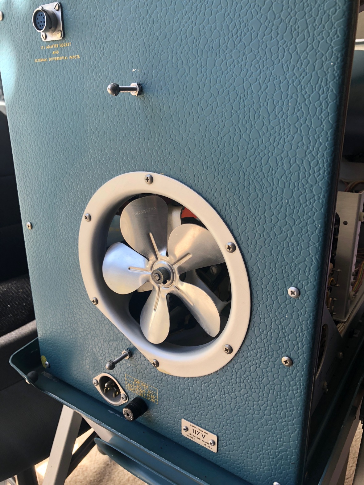
Time to get this boy working. First part which needs attention was the fan, which was stuck. Simple lubrication job was all it took.

Now coming to electrical restoration.
:SAFETY FIRST ::
DO NOT ATTEMPT TO REPAIR/OPEN/OPERATE/FOLLOW UNLESS YOU REALLY KNOW WHAT YOU ARE GETTING IN TO. THERE ARE DEADLY VOLTAGES INVOLVED AND IT CAN KILL YOU.
THERE ARE BETTER WAYS TO DIE IF YOU ARE UP TO THAT.
Even if you are familiar with electronics, be very careful when you work on something like this, a maximum potential difference of 650V DC is present in this equipment . -150V,+100V,+300 and >+400V unregulated are the DC power rails inside. DO TAKE CARE. CRT HV from cathode to anode is ~4000V.
Use test instruments with right attenuation probes, example, 10:1 probes or HV probes,else you may fry your test instrument & the signal generator.
This is a simple instrument compared to a 500 series oscilloscope, so its much easy. Quick round of visual inspection showed everything in good order, again signs of a well maintained equipment. The power rail is very simple here, just three voltages, -150V, +100 and +300V. The usual Tektronix 500 series design of -150V reference with 5651. One point to notice here is some older models used selenium rectifier. The rectifier assembly is behind the Fan unit, you can see it in the above picture. Mine had silicon diodes.
Capacitor Reforming
Now to capacitors. Since my HP 608C project I am experimenting more and more with reforming electrolytic capacitors, as they preserve the equipment aesthetics compared to recapping. I am not an advocate of re-cap or re-form. I do what I feel as best for the situation.
I am still exploring the pros and cons of the entire reforming exercise, so here is the second episode and findings on reforming capacitors.
Remember, do disconnect capacitor from circuit before reforming, check my HP 608C project for safety precautions and detailed procedure.
There are electrolytic caps on all rails. I have modified the version of schematic I used for 608C capacitor reforming, with the following changes.
- Lower value resistor to 10kΩ/2W, to charge the caps as close to the output voltage of the power supply – be very careful to increase the reforming voltage gradually.
- Reduce the reforming current – by slowing the rate at which voltage is applied – I settled at 500µA this time.
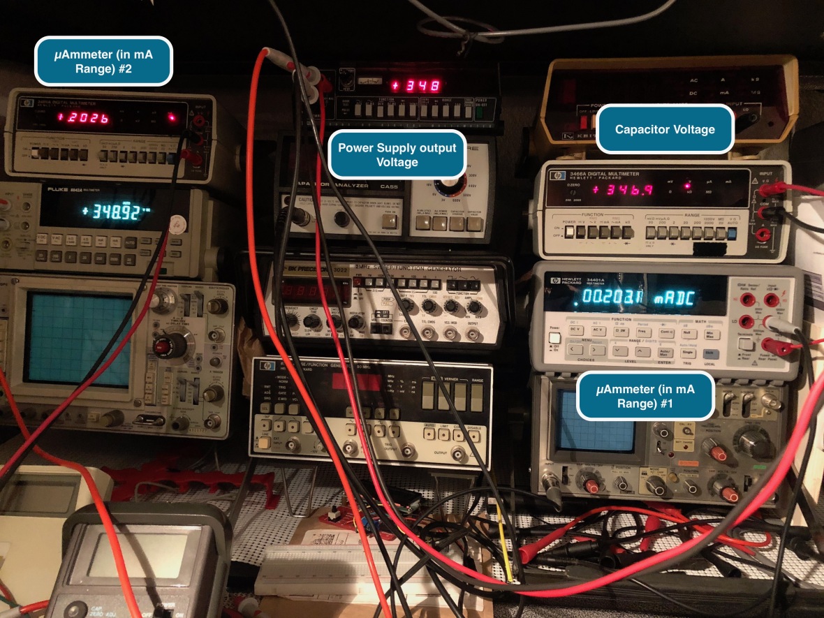
- One digital volt meter on the power supply output.
- One more digital µA in series, just in case my 34401A is not accurate.
New schematic is here –

Here are the results after reforming. Took approximately 15-20 minutes per capacitor to get the leakage current stable and low.
Here is an example, Capacitor – C620, 125µF/350V
202µA leakage current at 346V, ~ 2-3 minutes after applying the voltage. Also NO need to suspect my 34401A, vintage 4.5digit HP DMM is also reporting 202µA current.
Here is the results from a 47µF/450V modern KEMET. Its not a true comparison as there are differences in ratings (125µF vs 47µF and rated voltage 350V vs 450V) between both. Still it gives me an impression that the whole process is not bad.The reformed capacitor is back to life.

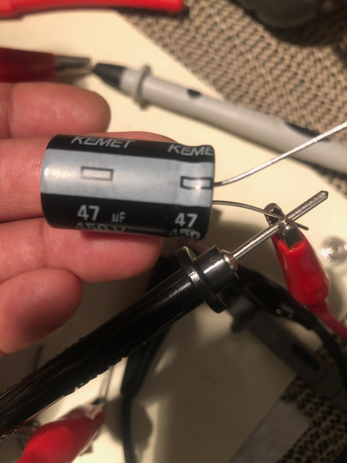
47µF/450V – 78µA leakage current at 438V, ~ 2-3 minutes after applying the voltage.
Lesson learned till now – there is no definite success or failure. It depends on the capacitor.
My rule as of now –
Keep the capacitor – if the leakage current is below 200µA after loading at rated voltage for ~2-3 minutes.
Replace – if it shows higher leakage current or leakage current is increasing during reforming
Here is a picture taken during the reforming
On this curve tracer, I was able to reform all electrolytic capacitors. There were no paper caps to replace. So this was a no-recapping restore/repair.
Hints for troubleshooting
Now all set to power up.Few quick tips from service manual.
Check resistance of power rail –

For me all rails were close to the specified range, 300V was 13.3kΩ instead of 16k, I could not find anything suspicious, so decided to go head.
In case you want to trace or verify power cabling, here is the color code. 
And for identification of components to function, here is the Component numbering scheme used – example

For example – V100/C101/R144 will be a tube/capacitor/resistor in step generator
Unlike 500 series scopes, there is no thermal delay, rather plate voltage is applied straight.
Tubes are mostly 6AU6 and 12AU6s. I haven’t seen them failing often, still tested all tubes. Even if you don’t test all the tubes, its a good idea to check the following ones.
- 6080 series pass in the power supply- V627
- 12B4A series pass in the power supply – V607 and V657
- 6AQ5 – in HV Oscillator – V810
- 6CG7 – H and V Amps – V484 and V384
- 5651 – VR Tube – V649
Everything checked good for me and I went straight to power on, with variac and monitoring all the power rails as always with meters. All rails came up well and here is the result with first transistor.

I did check and re-adjusted the calibration, most of it was intact, with very slight changes in limits.
Here are some more pictures taken from the unit at mid night, where I am active and working on these toys. Note: There is no Photoshop involved in these pictures, they are virgin, posted as it is from my phone camera, the metering point was was adjusted before clicking to get the right exposure.


Simple Diode Curve
And the NPN Curve

And this is how a PNP transistor trace looks. Its upside down 😉

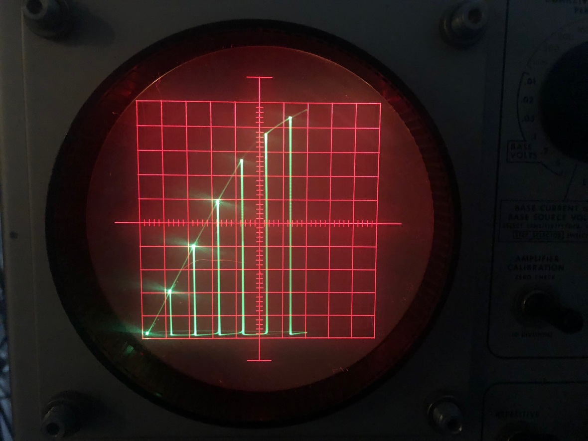
Measurements with 575 Curve Tracer
Lets do few quick characteristics measurements using 575. Lets take a simple one, of a VR tube like 5651, the grandfather of Zener. 5651 data is 87V at 3.5mA .
Here is how it looks when hooked on to 575. Settings – dissipation resistor ~5k/10k. horizontal volts/div at 20V and vertical current at 1mA/div.

You can see that 5651 fires around ~117 volts and regulates down to ~87, matching the tube data.
A neon lamp also gives the same trace as operationally it is also a VR Tube, much lower current though. Here is one.

Now lets read a NPN transistor hfe and hFE .
hfe is the AC voltage gain, β or β (ac) = Δic / Δib
hFE or β (dc) = Ic / Ib

As per the reading above for a Vce of 14V (to be precise the Vce of ~10v as the dissipation limiting resistor is at 200 Ω)
The hfe or β (ac) ~ is 4.6mA/20µA ~ 230
2N3904 typical datasheet specifies hfe from 100-400
Now to hFE
Point #1 – 17.4 mA/80µA ~ 217
Point #2 – 22 mA/100µA ~ 220
2N3904 typical datasheet specifies hFE from 80-300.
Now to experiment a bit , I tested the hFE on the transistor tester, and here is the result.

I tested the same transistor using a multi meter with transistor test capability, and it returns a hFE of 175.

Now this hFE as per these meters are a bit low, compared to 575. I know I am not making a perfect precise reading with 575 with 20V collector sweep.
In any case this I was curious to investigate why this difference. Of course there are errors on reading the data from 575 trace on a higher scale, so I zoomed in the 575 trace by changing the vertical scale.
So here is the hFE and hfe calculation with a Vce of 2V, vertical mA/div = 1mA
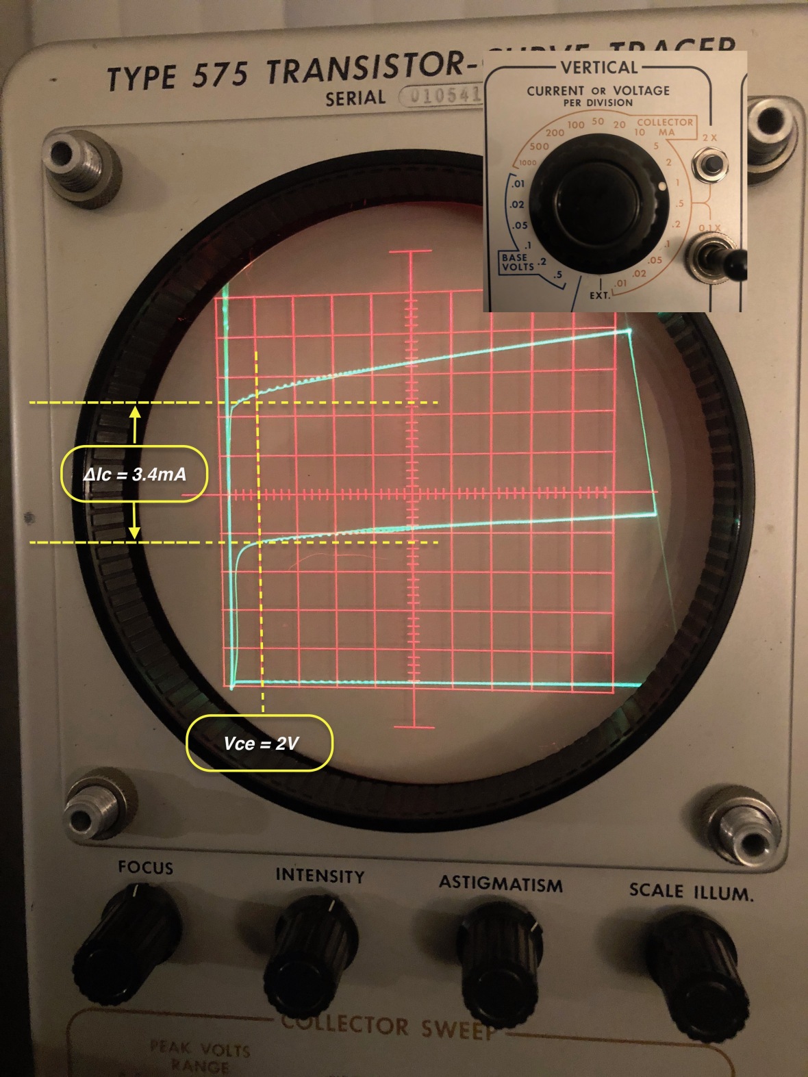
Since rest all parameters remain the same, for Vcc of 2V (~1.2V Vce as dissipation limiting resistor is at 200 Ω)
The hfe or β (ac) ~ is 3.4mA/20µA = 170.
Now to hFE
Point #1 – 3.8 mA/20µA = 190
Point #2 – 7.4 mA/40µA = 185
Now this hFE is close to what the generic digital measuring meters are reporting. If I reduce the horizontal scale to a lower value than 2V/div, I may get it closer. Basically the non linearity in β is what we see here.
To verify the Vce applied by the digital meters during testing, I decided to measure it.
HP 34401A was of help, in which you can enable the math function to store the minimum and maximum readings, and here is the result, when it was plugged across the collector and emitter while both the modern testers were testing the transistors.
Here is the maximum value from the µController based components tester. Maximum voltage across emitter and collector during the hFE testing is 2.8V.

I measured the voltage applied by the BK precision meter between collector and emitter as well during transistor test, and here is the result.
Maximum voltage across emitter and collector during the hFE testing is 3.08V.

This is an important point to note while using these testers. These instruments are expected to deliver a very small Vce. Not blaming them, they are designed for that purpose and does the job well too, to quickly tell you if a transistor is good or bad.
Off the topic, to highlight the components tester, it was developed by Markus Frejek and later enhanced by Karl-Heinz Kübbeler, and kits sold in thousands by Chinese websites as component tester. Original work – https://github.com/svn2github/transistortester – which really is an art of micro controller programming.
Coming back to the curve tracer, the hFE or so called current transfer characteristics can be directly plotted on the 575.This example uses 2N3904.
To do this you keep the vertical setting to Ic, but move the horizontal knob to base current/voltage and use the step generator to control the base current per step.

Another interesting curve to trace in a generic transistor is the Jim Williams pulse curve or back biased NPN avalanche curve or reverse bias avalanche curve for collector/base.
All settings remain the same, except – sweep range to 200v, and ensure a collector dissipation resistor of atleast 10K to keep the breakdown current to minimum. This is with +ve base setp, which is not the ideal Back Bias, rather a Vce breakdown in CE mode.


This is the complete reverse bias NPN Avalanche , same settings, but with -ve collector step too, for a higher breakdown voltage, but zero current before breakdown.


To wrap up, you could spend hours on this with one transistor, trying to understand the behavior. This is why you must have a Tektronix 575, a light weight, portable, and low power, compact curve tracer plus room heater, as you definitely wanna know the exact performance of a transistor or semiconductor or tube (with modifications ) for a practical design.
I
=== Z Modulation like Noise in Trace ==
11 Nov 2018,
John Sykes wrote to me after reading my post and pointed me to something very interesting,
On some of the pictures, the trace had some funny modulation or noise in them.
Observe the curlies in the trace.
He had same problem and he nailed it already and told me that it is an interference from mains.
I remember noticing this during the restoration and I was thinking about it, but even I am not sure where I lost track of the problem. I definitely was worried about it, but it slipped from my list of things to check.
John’s mail got me back in to the whole problem again, and I started tracing it and thanks to his pointer, I was able to proceed further without repeating what he already did.So it was just about fixing it. John had a solution in hand but I was more curious to trace the source of the problem.
Tried random tricks like more bypass caps, adding X/Y Cap in mains input, common mode choke, ferrite beads, power supply ripple check, praying to power supply gods, what not -still no luck that I decided to investigate properly.
So here is the first breakthrough. The problem happens ONLY at night.
Here is a trace at day time.

And all settings and transistor remains same, and here is the trace at night.
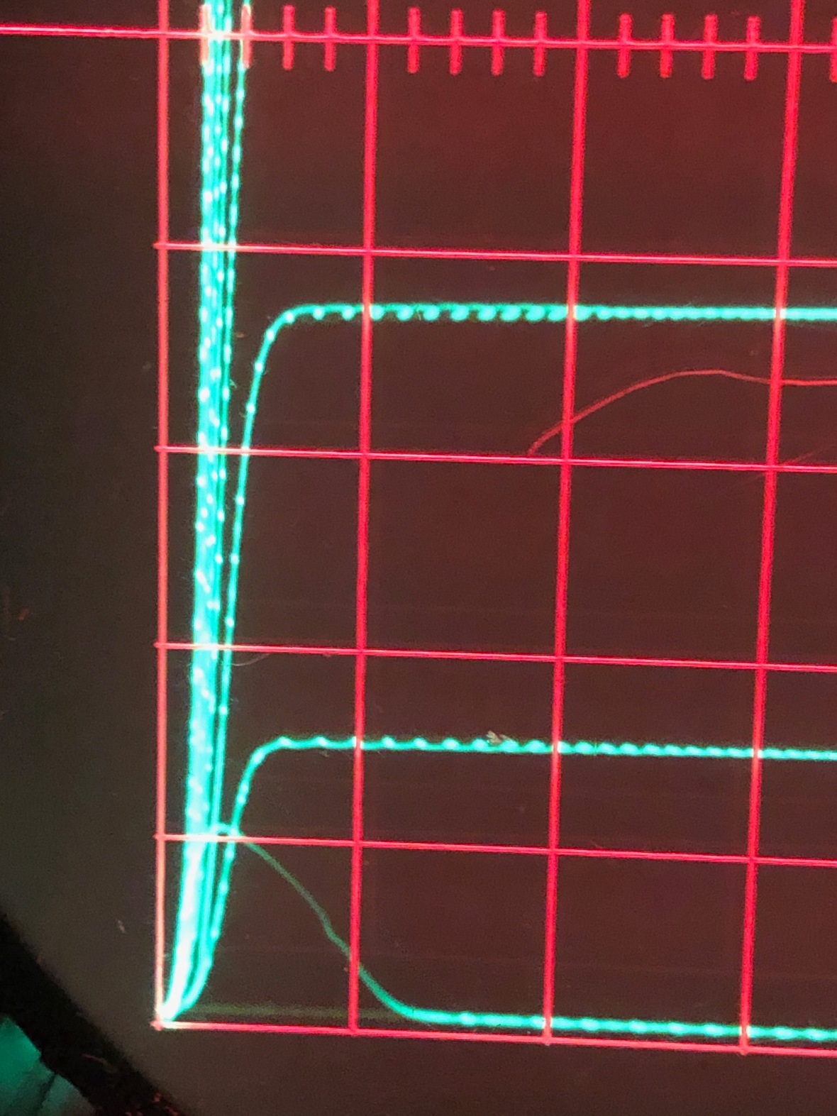
Investigation in to the collector sweep voltage showed incoming noise as John already discovered.
Here is the collector sweep wave

More of the actual sweep

And the zoomed in wave.
Now, I was trying to identify the spectrum of this, to either arrest it from getting in to the 575 or remove it from the source. Did a FFT of line voltage on my Agilent DSO. Even though the rough calculation of the offending signal turned out to be at around 10Khz-25Khz, nothing was visible in the FFT. I would not assume it to be really sensitive, or accurate either.
I was trying to measure the input to the sweep transformer to see the actual wave coming in . I was trying to take a picture of the Oscilloscope trace and it was not coming clear, so I decided to switch off the light in the room, came back to take the picture and observed this surprise in the collector sweep voltage.
With Light off –

And I switched the light On and here it is.

Totally by accident, I discovered the criminal behind all this –
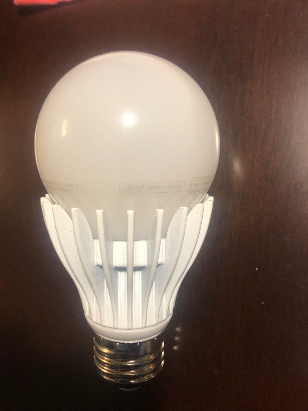

Another LED energy saving bulb. Edison, we love you 😉 This was not a purchase from ebay or from other cheap source, I am 100% sure I purchased it from one of the home depots or lowes or similar ones.
The fact which surprises me by the most is how noisy these things are and we really don’t know how badly they impact other electrical appliances at home. It may be good to bring in strict standards for electrical pollution, as we depend on power for everything.
I decided to leave 575 untouched, as it is not its fault. Thanks to John again for poking my brain with this.
Unanswered questions :-
Why this noise was not showing up in my Agilent DSO ? may be the FFT is not capable of catching it?
Or is there a possibility that the real interference signal gets some sort of resonance inside the sweep transformer ?
Moral of the story – a 1950s Tek is a clean machine, if you find noise, its externally injected.
I found the need for a spectrum analyzer to trace these things and I ended up scavenging this. All three are broken mostly needs fix (my brain too). My project for next year.

Disclaimer
I have no commercial affiliation with any of the products/organizations/individuals mentioned in this blog.
The information provided here is for educational purpose only.
You are free to distribute this as long as it stays original with all information as is here and it is free and you don’t scavenge any tubes from any scopes or this blog.
NO electrons were harmed during the repair/filming of this instrument restoration. All free electrons found inside the unit were rehabilitated to the nearest vacuum tube.
NO EXTRA SCREWS OR PARTS WERE OFFICIALLY FOUND AFTER REASSEMBLY. UNOFFICIAL EXTRA ITEMS WERE DISPOSED OFF SECRETLY AND DECLARED AS “EXCESSIVE ASSEMBLY” DURING MANUFACTURE.
Please do report any errors or stupidity.
=== THE END ===
For more restorations and experiments, Click here to get to homepage

One thought on “Tektronix 575 (Tek 575) Curve Tracer – Restore”